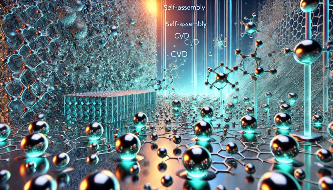
Nanoengineering has transformed how we create materials at the atomic and molecular levels. Among the leading techniques driving this revolution are self-assembly and chemical vapor deposition (CVD). These processes allow us to manipulate materials with unmatched precision, leading to breakthroughs in fields such as electronics, biotechnology, and renewable energy.
In this article, we’ll explore what these techniques are, how they work, and why they’re so important for advancing nanotechnology.
What is Self-Assembly?
Self-assembly is a fascinating process where nanoparticles or molecules spontaneously organize themselves into a structured pattern. Think of it like building a complex puzzle where the pieces naturally fall into place without you having to guide each one. The forces at play are often weak, like van der Waals forces, hydrogen bonding, and electrostatic interactions. However, when combined, these forces can lead to highly ordered nanostructures.
Self-assembly is common in nature. For example, DNA folds into precise structures, and proteins naturally form complex shapes. In nanoengineering, we replicate these natural processes to create materials that are functional and structured at the nanoscale.
Key Advantages of Self-Assembly in Nanoengineering
Self-assembly offers several unique benefits. Let’s look at why it’s such a game-changer in nanoengineering:
- Cost-Effective: You don’t need expensive machinery or a lot of human intervention. The process happens on its own, making it a cheaper option for large-scale manufacturing.
- High Precision: Once the system is set up, the final structure is incredibly precise. The accuracy is often at the atomic level, which is crucial for many high-tech applications.
- Scalability: Self-assembly works well for both small-scale lab experiments and large-scale industrial production. You can apply it across various fields, from drug delivery to electronics.
However, like any technology, self-assembly has its challenges.
Challenges with Self-Assembly
While self-assembly sounds like the perfect solution, it isn’t without its obstacles. Achieving the desired precision in all scenarios can be tricky. The process often relies on environmental factors like temperature, pressure, and solvent choice, which can introduce unpredictability. Additionally, controlling the size and alignment of assembled structures is not always straightforward. Despite these challenges, self-assembly remains a powerful tool for creating nanomaterials.
What is Chemical Vapor Deposition (CVD)?
Now, let’s talk about Chemical Vapor Deposition (CVD). This technique allows us to deposit thin films of materials onto a substrate. CVD works by exposing the substrate to gaseous precursors, which react to form solid materials that coat the surface.
The beauty of CVD lies in its versatility. It can be used to deposit a wide range of materials, including metals, semiconductors, and insulators. Moreover, CVD is capable of producing highly uniform coatings with excellent control over thickness, making it ideal for fabricating components in electronics, solar cells, and advanced sensors.
Types of CVD
There are several variations of CVD, each with its own advantages:
- Low-Pressure CVD (LPCVD): Uses lower pressures to achieve better control over the deposition process. It’s commonly used in semiconductor manufacturing.
- Plasma-Enhanced CVD (PECVD): Involves using plasma to enhance chemical reactions at lower temperatures. This is particularly useful when working with materials that are sensitive to high temperatures.
- Metal-Organic CVD (MOCVD): Involves metal-organic compounds as precursors. It is widely used in the production of high-quality films for LEDs and solar cells.
Each of these types has its own application, but all offer the benefits of high precision, uniformity, and scalability.
Applications of Self-Assembly and CVD in Nanoengineering
Both self-assembly and CVD find extensive use in various fields of nanoengineering. Below is a table highlighting some common applications:
| Technique | Application | Key Benefits |
|---|---|---|
| Self-Assembly | Nanostructured materials (e.g., nanoparticles, nanowires) | Cost-effective, scalable, precise |
| Self-Assembly | Drug delivery systems | High precision, biocompatibility |
| CVD | Semiconductor manufacturing (e.g., transistors, solar cells) | Uniform coatings, high-quality films |
| CVD | Thin-film deposition in sensors and LEDs | High uniformity, scalability |
| CVD | Carbon nanotube synthesis | Tailored properties, versatile use |
Both techniques are pivotal for creating the next generation of electronic devices, materials, and even life-saving medical applications.
How Do Self-Assembly and CVD Complement Each Other?
Self-assembly and CVD may seem like separate techniques, but they can actually complement each other in exciting ways. For instance, CVD can be used to grow thin films or nanostructures onto a substrate that was pre-patterned using self-assembly. This synergy opens up even more possibilities for designing materials with complex, multi-layered structures.
In some applications, researchers use CVD to create the base layer, followed by self-assembly to fine-tune the top layer. This combination ensures the final product has both high performance and intricate designs. Think of it like starting with a solid foundation and adding intricate details that make the structure unique and functional.
The Future of Nanoengineering with Self-Assembly and CVD
The future of nanoengineering looks incredibly promising. Both self-assembly and CVD will continue to play a significant role in pushing the boundaries of what’s possible. As technology improves, these methods will likely become more efficient, allowing for even more precise control over nanoscale materials.
The integration of self-assembly with CVD will lead to even more sophisticated structures, opening up new possibilities in areas such as quantum computing, nanomedicine, and advanced energy storage systems. Researchers are already exploring new materials that could revolutionize industries, from electronics to sustainable energy.
Conclusion
Self-assembly and Chemical Vapor Deposition (CVD) are two of the most important techniques in the world of nanoengineering. Self-assembly provides a low-cost, scalable method for creating precise nanostructures, while CVD allows for high-quality, uniform thin films that are essential for modern technology. Together, these methods are advancing fields like electronics, energy, and medicine, offering exciting possibilities for the future. As both techniques evolve, we can expect even more groundbreaking innovations at the nanoscale.

